- 您现在的位置:买卖IC网 > Sheet目录1995 > HI5746KCB-T (Intersil)CONV A/D 10BIT 40MSPS 28-SOIC
4
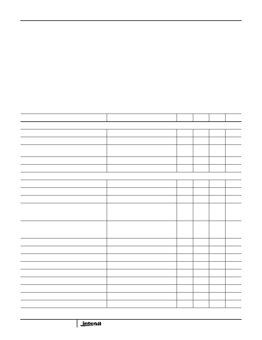
Absolute Maximum Ratings TA = 25oC
Thermal Information
Supply Voltage, AVCC or DVCC to AGND or DGND . . . . . . . . . . .6V
DGND to AGND . . . . . . . . . . . . . . . . . . . . . . . . . . . . . . . . . . . . . 0.3V
Digital I/O Pins . . . . . . . . . . . . . . . . . . . . . . . . . . . . . DGND to DVCC
Analog I/O Pins . . . . . . . . . . . . . . . . . . . . . . . . . . . . .AGND to AVCC
Operating Conditions
Temperature Range
HI5746KCB (Typ) . . . . . . . . . . . . . . . . . . . . . . . . . . . . 0oC to 70oC
Thermal Resistance (Typical, Note 1)
θ
JA (
oC/W)
SOIC Package . . . . . . . . . . . . . . . . . . . . . . . . . . . . .
70
SSOP Package . . . . . . . . . . . . . . . . . . . . . . . . . . . .
100
Maximum Junction Temperature . . . . . . . . . . . . . . . . . . . . . . . 150oC
Maximum Storage Temperature Range . . . . . . . . . .
-65oC to 150oC
Maximum Lead Temperature (Soldering 10s) . . . . . . . . . . . . . 300oC
(SOIC, SSOP - Lead Tips Only)
CAUTION: Stresses above those listed in “Absolute Maximum Ratings” may cause permanent damage to the device. This is a stress only rating and operation of the
device at these or any other conditions above those indicated in the operational sections of this specification is not implied.
NOTE:
1.
θ
JA is measured with the component mounted on an evaluation PC board in free air.
Electrical Specifications
AVCC = DVCC1 = 5.0V; DVCC2 = 3.0V, VREF+ = 2.5V; VREF- = 2.0V; fS = 40 MSPS at 50% Duty Cycle;
CL = 10pF; TA = 25
oC; Differential Analog Input; Typical Values are Test Results at 25oC,
Unless Otherwise Specified
PARAMETER
TEST CONDITIONS
MIN
TYP
MAX
UNITS
ACCURACY
Resolution
10
-
Bits
Integral Linearity Error, INL
fIN = DC
-
±1.0
±2.0
LSB
Differential Linearity Error, DNL
(Guaranteed No Missing Codes)
fIN = DC
-
±0.5
±1.0
LSB
Offset Error, VOS
fIN = DC
-40
12
40
LSB
Full Scale Error, FSE
fIN = DC
-
4
-
LSB
DYNAMIC CHARACTERISTICS
Minimum Conversion Rate
No Missing Codes
-
0.5
1
MSPS
Maximum Conversion Rate
No Missing Codes
40
-
MSPS
Effective Number of Bits, ENOB
fIN = 10MHz
8.55
8.8
-
Bits
Signal to Noise and Distortion Ratio, SINAD
fIN = 10MHz
53.2
54.9
-
dB
Signal to Noise Ratio, SNR
fIN = 10MHz
53.2
55.4
-
dB
Total Harmonic Distortion, THD
fIN = 10MHz
-
-64.6
-
dBc
2nd Harmonic Distortion
fIN = 10MHz
-
-67.8
-
dBc
3rd Harmonic Distortion
fIN = 10MHz
-
-68.3
-
dBc
Spurious Free Dynamic Range, SFDR
fIN = 10MHz
-
67.8
-
dBc
Intermodulation Distortion, IMD
f1 = 1MHz, f2 = 1.02MHz
-
64
-
dBc
Differential Gain Error
fS = 17.72 MSPS, 6 Step, Mod Ramp
-
0.8
-
%
Differential Phase Error
fS = 17.72 MSPS, 6 Step, Mod Ramp
-
0.1
-
Degree
Transient Response
(Note 2)
-
1
-
Cycle
Over-Voltage Recovery
0.2V Overdrive (Note 2)
-
1
-
Cycle
RMS Signal
RMS Noise + Distortion
--------------------------------------------------------------
=
RMS Signal
RMS Noise
-------------------------------
=
HI5746
发布紧急采购,3分钟左右您将得到回复。
相关PDF资料
HI5760BIBZ
CONV D/A 10-BIT 125MSPS 28-SOIC
HI5762/6IN
CONV A/DDUAL 10BIT 60MSPS 44MQFP
HI5766KCB
CONV A/D 10BIT 60MSPS 28-SOIC
HI5767/6IB
CONV A/D 10BIT 60MSPS 28-SOIC
HI5805BIB
IC ADC 12-BIT 5MSPS 28-SOIC
HI5812JIBZ-T
ADC 12BIT SAMPL TRK&HOLD 24-SOIC
HI5828IN
DAC DUAL 12BIT 130MHZ 48-LQFP
HI5860IBZ
CONV D/A 12-BIT 130MSPS 28-SOIC
相关代理商/技术参数
HI5746KCBZ
功能描述:模数转换器 - ADC 28 COMTEMP A/D 10BIT 40MSPS RoHS:否 制造商:Texas Instruments 通道数量:2 结构:Sigma-Delta 转换速率:125 SPs to 8 KSPs 分辨率:24 bit 输入类型:Differential 信噪比:107 dB 接口类型:SPI 工作电源电压:1.7 V to 3.6 V, 2.7 V to 5.25 V 最大工作温度:+ 85 C 安装风格:SMD/SMT 封装 / 箱体:VQFN-32
HI5746KCBZ-T
功能描述:模数转换器 - ADC HI5746KCB IN TAPE RoHS:否 制造商:Texas Instruments 通道数量:2 结构:Sigma-Delta 转换速率:125 SPs to 8 KSPs 分辨率:24 bit 输入类型:Differential 信噪比:107 dB 接口类型:SPI 工作电源电压:1.7 V to 3.6 V, 2.7 V to 5.25 V 最大工作温度:+ 85 C 安装风格:SMD/SMT 封装 / 箱体:VQFN-32
HI-574A
制造商:INTERSIL 制造商全称:Intersil Corporation 功能描述:Complete, 12-Bit A/D Converters with Microprocessor Interface
HI-574A_01
制造商:INTERSIL 制造商全称:Intersil Corporation 功能描述:Complete, 12-Bit A/D Converters with Microprocessor Interface
HI-574A_08
制造商:INTERSIL 制造商全称:Intersil Corporation 功能描述:Complete, 12-Bit A/D Converters with Converters with Microprocessor Interface
HI5760
制造商:INTERSIL 制造商全称:Intersil Corporation 功能描述:10-Bit, 125/60MSPS, High Speed D/A Converter
HI5760/6IA
制造商:INTERSIL 制造商全称:Intersil Corporation 功能描述:10-Bit, 125/60MSPS, High Speed D/A Converter
HI5760/6IB
功能描述:IC DAC 10-BIT 60MSPS 28-SOIC RoHS:否 类别:集成电路 (IC) >> 数据采集 - 数模转换器 系列:- 标准包装:2,400 系列:- 设置时间:- 位数:18 数据接口:串行 转换器数目:3 电压电源:模拟和数字 功率耗散(最大):- 工作温度:-40°C ~ 85°C 安装类型:表面贴装 封装/外壳:36-TFBGA 供应商设备封装:36-TFBGA 包装:带卷 (TR) 输出数目和类型:* 采样率(每秒):*